研究目的
Investigating the laser micro-drilling of via holes in Si, InP, and InSb semiconductor wafers using a 1070 nm wavelength fibre laser with millisecond pulse widths.
研究成果
The study demonstrated the ability to rapidly drill through hundreds of microns of material to create and locate a hole of sub-mm dimensions precisely in brittle semiconductor wafers using a 1070 nm wavelength fibre laser. The relative dimensions of the holes were not simply related to the thermal diffusivity of each single crystal semiconductor material. Future work will investigate the requirements for the epitaxial structure or surface passivation of the hole.
研究不足
The study did not account for the thermal diffusivity of the materials and the extent of the area affected by rapid surface heating in its simple model. Future work will investigate the requirements for the epitaxial structure or surface passivation of the hole.
1:Experimental Design and Method Selection:
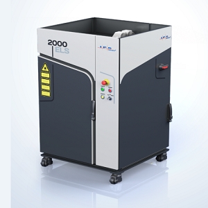
The study used an IPG Laser Model YLR-2000 CW multimode 2 kW Ytterbium Fibre Laser and a JK400 (400 W) fibre laser, both with 1070 nm wavelength, to drill micro-holes in Si, InP, and InSb semiconductor wafers. The methodology involved varying principal drilling parameters such as power, pulse length, focal position, and wafer orientation.
2:Sample Selection and Data Sources:
High-quality single crystal wafer substrates suitable for epitaxial growth were used, with a polished front surface roughness of 2 nm and wafer thickness in the range of 300 μm to 500 μm.
3:List of Experimental Equipment and Materials:
The equipment included an IPG YLR-2000 CW multimode 2 kW Ytterbium Fibre Laser, a JK400 (400 W) fibre laser, optical microscopy (Nikon Eclipse LV100ND or an Olympus MX51), and a precision translation stage.
4:Experimental Procedures and Operational Workflow:
Substrates were placed with the highly-polished face a few degrees from the normal to the laser beam, which was focused on the substrate surface. An assist gas of Ar was used in all experiments.
5:Data Analysis Methods:
Optical microscopy and cross-sectional analysis were used to quantify hole dimensions and the distribution of recast material.
独家科研数据包��,助您复现前沿成果���,加速创新突破
获取完整内容


