研究目的
To obtain narrow linewidth semiconductor laser around 1564 nm using a simple method for large-scale production.
研究成果
A narrow linewidth DBR semiconductor laser based on HOBGs structure was developed, achieving a wavelength peak of 1564nm, output power of 9.9 mW, SMSR more than 30 dB, and a linewidth of 70 KHz. The method avoids the high cost and low yield problem of complex lithography technologies, providing a simple solution for large-scale production.
研究不足
The high-order scattering loss due to HOBGs structure increases the threshold current and reduces the output power and slope efficiency. The grating trench cannot be over-etched to avoid high order scattering enhancement.
1:Experimental Design and Method Selection:
The DBR laser with high-order Bragg gratings (HOBGs) was designed using the commercial software COMSOL Multiphysics. The grating parameters were calculated to achieve narrow linewidth emission.
2:Sample Selection and Data Sources:
The laser was fabricated on a n-InP substrate with a vertical structure consisting of various layers grown by metal-organic chemical vapor deposition (MOCVD).
3:List of Experimental Equipment and Materials:
i-line lithography technology was used for grating definition, inductively coupled plasma etching (ICP) for grating etching, and plasma enhanced chemical vapor deposition (PECVD) for silica layer deposition.
4:Experimental Procedures and Operational Workflow:
The process included grating definition, etching, ridge waveguide creation, passivation, metallization, and chip cleaving. The laser was then packaged into a temperature control module for testing.
5:Data Analysis Methods:
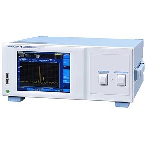
The spectral linewidth was characterized using the power spectral density method, and the frequency noise was measured by an OE4000 cross-correlation homodyne phase/frequency noise automatic test system.
独家科研数据包����,助您复现前沿成果,加速创新突破
获取完整内容