研究目的
To demonstrate a narrow-strip single-longitudinal-mode gain-coupled distributed feedback semiconductor laser with a central wavelength of approximately 670 nm, fabricated using a novel micro-scale regrowth-free gain-coupled grating with an island-like shape without nanoscale gratings by i-line lithography only.
研究成果
The study successfully demonstrates a narrow-strip single-longitudinal-mode gain-coupled DFB semiconductor laser with a central wavelength of approximately 670 nm. The laser achieves good performance with a maximum output power of 48.1 mW and a slope efficiency of 0.79 W/A. The device shows potential for applications in lithium atom detection and other areas requiring stable, single-longitudinal-mode lasers.
研究不足
The study does not address the long-term reliability of the fabricated lasers under continuous operation. The fabrication process, while simpler than previous methods, still requires precise control over lithography and etching parameters.
1:Experimental Design and Method Selection:
The study involves the fabrication of a gain-coupled DFB semiconductor laser using i-line lithography and conventional ICP etching. The design includes periodic anodes injection to achieve a gain coupling mechanism.
2:Sample Selection and Data Sources:
The samples are fabricated on AlGaInP/GaInP quantum wells emitting at 670 nm.
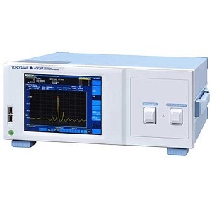
3:List of Experimental Equipment and Materials:
Includes i-line lithography equipment, ICP etcher, MOCVD for epitaxial growth, and a YOKOGAWA AQ6370C spectrum analyzer for measurements.
4:Experimental Procedures and Operational Workflow:
The process involves deposition of an island-like photoresist layer, etching to form periodic island-like trenches, deposition of silica for insulation, and formation of periodic metal p-contact.
5:Data Analysis Methods:
The performance of the laser is analyzed based on output power, slope efficiency, and side-mode suppression ratio.
独家科研数据包,助您复现前沿成果�,加速创新突破
获取完整内容